| Navigation | |
FPGA implementation of a NavIC-disciplined 10MHz reference for SATCOM networks
We have implemented the circuit design comprising of phase detector, limiter, loop filter, NCO and clock divider in hardware using FPGA. The disciplined 10MHz is measured to have a long term (10,000 sec) stability of 1.7 x 10⁻¹⁰. In case of non-availability of NavIC 1PPS, the circuit is designed to work with an internal 1PPS signal. |
 |
|
 |
|
 |
|
 |
|
Introduction
Satellite communication network can be established using microwave signals with accurate, stable and low noise frequencies. Many frequency-based devices with independent local oscillators are used in an Earth Station to generate and convert carrier frequencies and modulate/demodulate data. Even RF measurement instruments like Frequency Counters, Signal generators, Spectrum Analyzers have reference oscillators that need periodic calibration. It is essential to connect these instruments to a common reference, with low phase noise and long term stability of an atomic frequency standard in order to minimize frequency drift issues and for supporting higher data rates [1][2].
SATCOM networks generally use the GPS 1PPS signal for synchronization. The motivation of this work is to design and develop a circuit to generate a 10 MHz reference output derived from the NavIC 1PPS signal as the primary reference, thus reducing the dependency on a foreign system for an assured indigenous system guaranteed to be available to Indian users.
The organization of the paper is as follows. Section II explains the design and implementation of the proposed disciplining circuit. Test results are presented in section III along with a discussion, with section IV concluding the paper.
FPGA design and implementation
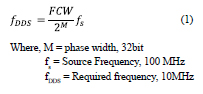
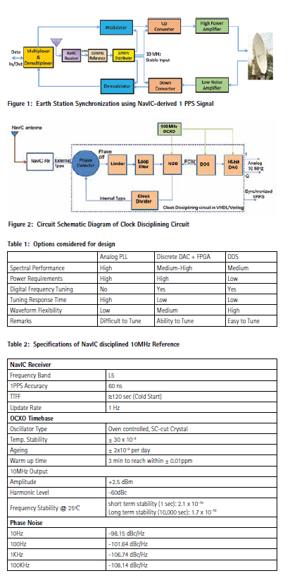
For the synchronization of an Earth Station, a typical scheme uses a GNSS (NavIC) receiver to derive the timing solution in the 1 PPS format, which is then used to obtain the desired 10MHz stable input (see Figure 1). The disciplining 10MHz using NavIC 1 PPS signal is based on a phase detector to sense the difference of it from internal 1 PPS derived from a local OCXO (as in figure 2). The phase frequency detector (PD) measures the phase and frequency difference between the external NavIC 1PPS clock reference and the internally generated 1PPS from the Numerically Controlled Oscillator (NCO)[3], [4].
In this design, phase-lock detection using a magnitude comparator and a re-triggerable counter is implemented in VHDL. The magnitude comparator measures error count of the limiter. The counter counts down when the error count is less than a fixed threshold value. It is retriggered if the error count exceeds the threshold.
Phase detector (PD) works on the principle of comparing the timing relationship between the internal and external signals to increase and decrease the Frequency Control Word (FCW).
Case 1 ensures that Frequency Control Word (FCW) does not change when the phase/frequency difference is zero,
Case 2 increases the frequency of the digital oscillator when the external timing signal leads the internal signal and
Case 3 decreases the frequency of the digital oscillator when the external timing signal lags the internal signal.
The 32 bit FCW controls the output frequency of the DDS as per the equation [5]:
A limiter is used to adjust the frequency of the digital oscillator arising from initial phase errors. The limiter limits the amount of change applied to the FCW of the digital oscillator per period of the external timing signal. Following the limiter is a loop filter which is a discrete standard filter and the digital oscillator is implemented using a DDS IP core. The FCW controls the frequency of the DDS, which is an accumulator (integrator) that adds the phase error output of the filter to itself. The digital output from the DDS is converted to analog using a 16-bit Dual channel DAC providing In phase (I) and Quadrature phase (Q) analog outputs with a 900 phase shift.
To generate disciplined 10MHz analog signal, different techniques like Direct Digital Frequency Synthesizer (DDS), Phase Lock loop (PLL), Clock generators on FPGA to dynamically program the output of a DAC etc. were considered. The best option of using DAC interfaced with FPGA was considered as per the comparative assessment shown in Table 1 [6].
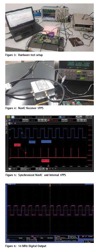
Specifications for the NavIC-Disciplined 10MHz reference are identical to the existing (GPS-based) system and are given in Table 2. FPGA implementation in sync with NavIC 1PPS was realized using NavIC Receiver [7] and COTS hardware viz., Kintex KC705 FPGA [8], FMC-150 (dual, 16-bit D/A) [9] and 100MHz OCXO [10] (Figure 3). The DDS IP core in FPGA and a Discrete DAC were used to generate a sinewave output with a specified frequency of 10MHz and phase (adjustable at runtime). The FMC-150 Daughter card has two 16-bit D/A Channels which give output in the range of 1V p-p.
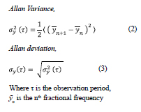
The single band 11 channel NavIC SPS receiver based on ASIC (Figure 4) is fabricated by ISRO’s 180nm CMOS foundry located at SCL Chandigarh. It has an acquisition and tracking sensitivity of 36 dBHz and 28 dBHz respectively with a 1PPS accuracy of around 60 ns.
Results and discussion
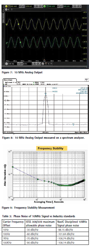
The synchronized 1 PPS FPGA output derived from NavIC indicates a coincidence with the trailing edge of the pulses (Figure 5). The corresponding 10MHz Digital and Analog outputs provide the desired waveforms (Figures 6 & 7) with a power level of +2.5dBm (Figure 8). The power consumption at the hardware in steady state is 5.71 W.
Frequency stability of clock, oscillators is measured using two-sample variance, the Allan variance (AVAR) method as represented in equation (2) & (3) [11]. The frequency stability of 10 MHz output is recorded (in CSV) using a frequency counter [12] with 12 digits/sec resolution and then processed using MATLAB code. The obtained stability values arrived at from the Allan deviation [12] plot show excellent performance (figure 9).
Where τ is the observation period, ȳn is the nth fractional frequency average over observation time τ.
The Intelsat Earth Station Standards IESS 308/309 [13], [14], [15] are adopted for the maximum acceptable phase noise levels in Earth stations. By designing systems which comply to these standards, the system reliability and interoperability could be assured. The disciplined output phase noise results are seen to be clearly better than these industry-specified standards (see table 3).
The disciplining process calibrates the oscillator by continuously compensating for the, frequency drift, environment effects and aging. In case of nonavailability of the NavIC 1 PPS, the long-term stability of the output follows that of the 100MHz OCXO.
Conclusion
NavIC 1 PPS signal was used to discipline a 100MHz OCXO frequency source to generate a reference frequency output of 10MHz. Implementation was carried out using Kintex KC705 FPGA, FMC- 150 DAC board, 100MHz OCXO and in-house developed NavIC Receiver. The disciplined 10MHz output has a short term (1 sec) stability of 2.1 x 10⁻¹⁰ and a long term (10,000 sec) stability of 1.7 x 10⁻¹⁰ with phase noise better than Industry-standards. The 10MHz signal was fed as an external reference to Kaband LNBC (Ka-L down converter in downlink chain) and Spectrum Analyzer, with both the setups performing well giving the expected outputs.
Acknowledgements
Acknowledgements are due to Director SAC, Associate Director SAC and Deputy Director SSAA for their motivational support, encouragement and Mr. Rakesh Kumar Bijarniya, Mr. Wikneswaran Pillai and Ms Anita Panday for guidance related to programming. The authors would also like to acknowledge support from various members of Technology Development Program team at SAC.
References
[1] https://www.furuno.com/en/gnss/ case/communitybroadcasting
[2] “Introduction to Timing and Synchronisation”, White Paper, Chris Farrow, Chronos Technology.
[3] https://github.com/dfannin/gpsdo
[4] https://en.wikipedia.org/wiki/ GPS_disciplined_oscillator
[5] “Direct Digital Synthesizer IP Core”, Martin Kumm, December 2008.
[6] “DDS Devices Generate High- Quality Waveforms Simply, Efficiently, and Flexibly.” Brendan Cronin, Analog Dialogue 46-01, January (2012).
[7] https://www.isro.gov.in/ sites/default/files/irnss_sps_ icd_version1.1-2017.pdf
[8] KC705 Evaluation Board User Guide, UG810 (v1.7) July 8, 2016
[9] FMC150 User Manual, Abaco systems, July 2013.
[10] http://www.andhraelec. com/httpdocs/catalogue/ OCXO%202055.pdf
[11] https://en.wikipedia.org/ wiki/Allan_variance
[12] https://www.keysight.com/ in/en/assets/7018-02642/ data-sheets/5990-6283.pdf
[13] https://itso.int/wp-content/ uploads/2018/04/Intelsat- ITSO-Trinidad-Earthstation- equipment.pdf
[14] http://www.intelsat.com/wp-content/ uploads/2017/03/IESS-308E11.pdf
[15] http://www.intelsat.com/wp-content/ uploads/2017/03/IESS-309E.pdf


 (No Ratings Yet)


Leave your response!