| GNSS | |
An open GNSS receiver platform architecture
|
||||
|
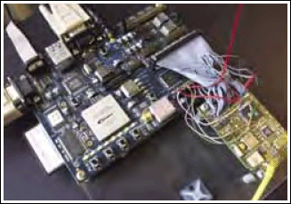
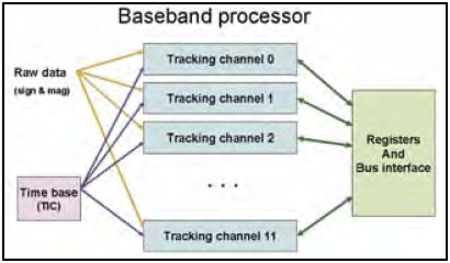
In early 2004 a plan was hatched to develop a Global Navigation Satellite System (GNSS) receiver based around Field Programmable Gate Array (FPGA) technology as a platform to support research in this fi eld. A joint project was set up between the School of Surveying and Spatial Information Systems (SISS) at the University of New South Wales and the National ICT Australia (NICTA), and soon after a small team was established. The team consisted of Kevin Parkinson, a post-graduate student at SISS with experience in FPGA and circuit board design, Frank Engel, a researcher with NICTA with software, Real Time Operating Systems (RTOS) and VHDL design knowledge and me, Peter Mumford from the SISS GNSS research group. At the end of the project we hoped to have an L1 GPS receiver running on a custom circuit board with the baseband processor and navigation solution processor running on an FPGA chip. The project is coming to an end now, and in this article, I will describe our design path, what has been achieved to date and then some potential research areas, but fi rst a little background. BackgroundThe Global Positioning System (GPS) is the only fully operational GNSS, In the near to medium-term future the market for satellite navigation technology is expected to continue to experience major growth (Canalys, 2004). The ability to integrate GNSS functionality into a device by hosting the baseband processor on an existing FPGA chip may provide an opportunity to lower costs, as well as providing a degree of future-proofi ng. In addition, the relative ease of creating special GNSS attributes in an FPGA may lead to novel applications or solve particular problems. The aim of the project is to develop a platform for supporting GNSS research and provide an accessible IP block. To explain the content of this platform, I will fi rst describe the three major components of a generic GNSS receiver, they are: 1) The RF front-end for receiving GNSS signals and converting it down into an Intermediate Frequency (IF) sampled baseband signal. 2) The baseband processor (sometimes called the correlator block) that 3) A micro-processor that runs software to control the baseband processor, and compute and communicate the position/time solution. The first component generally requires special circuitry, although single The Mitel GPS ArchitectThe Mitel GPS Architect (sometimes referred to as Orion) software was designed to help Mitel sell GPS chips by providing reference software in Altera ToolsThe FPGA vendor Altera provides a logic development tool called “Quartus” and a software development tool, the “NiosII IDE” for the NiosII soft-core processor. Quartus contains the “SOPC Builder” used for generating Nios core FPGA design fi les. The NiosII development tools provide a Hardware Abstraction Layer (HAL) and an Application Programming Interface (API) that incorporates the Newlib ANSI C embedded library. Altera has a range of development boards available, these are very convenient for getting projects up and running quickly. The Statix development board is used for the fi rst task of this project. Design ApproachThe approach we have taken is to break the development process into three main tasks. These tasks are identifi ed as “SuperStar_ NIOS”, “FPGA_baseband” and the “Custom GNSS Platform” and are described below. SuperStar-NIOSThis fi rst task involved porting the Mitel GPS Architect software to the NiosII processor. To set up the hardware for working on the port, we hacked into a Superstar receiver and removed the ARM60 and memory chips. We then connected the GP2021 address, data and control lines to a header onto an Altera Nios Development Board. Figure 1 shows what it looked like. There are signifi cant differences between the NiosII and ARM7 architectures and instruction sets, as well as differences in the development tools and embedded libraries. The main effort in porting the software concentrated around the RTOS, serial port communication and hardware initialization. The GPS Architect has a minimal RTOS closely integrated with the rest of the code. The task-switching core of this RTOS is coded in assembler, and this was completely rewritten for the NiosII processor. Some ‘glue logic’ was required to connect the Nios processor to the GP2021 baseband processor. After some debugging we obtained the correct position/time solution. However, the hardware arrangement was quite noisy, and the position solution revealed some evidence of this, however in most respects the receiver performed much like the Signav receiver running the GPS Architect. FPGA_basebandThe second task was to develop a baseband processor design in VHDL logic. The Zarlink 2021 was used as an architectural model to get things |
||||
Pages: 1 2


 (No Ratings Yet)


