| GNSS | |
Design methods for RF part of GNSS software receivers
|
||||
|
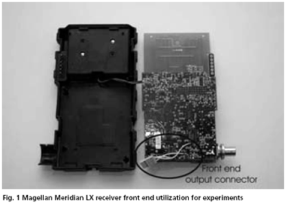
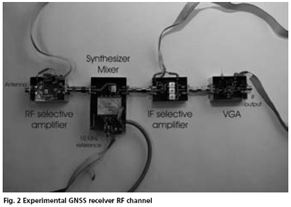
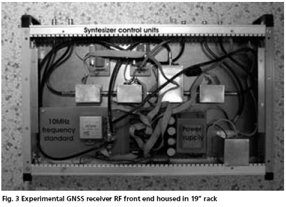
Many researchers and R&D laboratories in the world deal with the design of the software-based or experimental GNSS receivers using digital signal processing for work and experiments with received navigational signals. These concepts have one in common: the necessity of use of some analogue RF part before conversion of the signal to the digital domain. The problem of the RF front end design of the experimental or special purpose navigation receivers has to be solved. It is not an easy task as can be seen from many papers and conference contributions. The aim of this paper is analysis of the possibility of such GNSS RF front end design. We will discuss the following three main approaches: Technical requirements and characteristics of the experimental receiver RF front end come from the research aims. In this design phase the designer has to define the parameters like Experimental versus lot manufacture receiversThe requirements on RF front end of the experimental GNSS receiver are rather different than requirements on RF front end of the commonly The bandwidth of the common production receiver depends on its type. Low cost low power consumption GPS receivers use low sampling frequencies and bandwidth of about 2 MHz. These receivers usually have not implemented any multipath mitigation algorithms. The bandwidth of the high performance lot manufacture GPS receivers is much wider, i.e. 8 – 16 MHz. The bandwidth of the experimental receivers depends on the receiver mission. Typically, the bandwidth of such receiver should be adjustable in wide range to support broad spectrum of experiments. The frequency plan of the lot manufacture receivers is optimized from many aspects. The all required frequencies used for frequency conversion, signal sampling, and processing should be derived from one low cost high stability frequency standard. The power consumption of this frequency source should be kept low. Therefore most RF ASICs use only one synthesizer, which directly generates signals of the first local oscillator. The remaining frequencies are derived from this signal by dividers. This approach leads for utilization of the non standard intermediated frequencies. It is not problem for mass market products, where the special IF filters and frequency standard of required frequency are developed and produced for particular chip sets. The filters are usually manufactured by lot manufacture low cost SAW technology. In the case of experimental GNSS receivers, the development and production of the specialized components in the same manner as in the case of lot manufacture is very expensive. Therefore the standard RF components and integrated circuits should be used. The power consumption of the experimental receiver, cost and count of the components are not critical measures. It is appropriate to use common frequency standard and standard intermediated frequency. Nevertheless, the design of the synthesizers for experimental receivers is more complicated. Lot manufacture receiver front endThe easiest and cheapest way how to develop RF front end for GPS/ GNSS signal experimentation is an utilization of the RF front end of the lot manufacture GPS receiver. The most modern GPS receivers consist of at least two chips or blocks, RF ASIC and IF DSP ASIC. The signal on the RF ASIC output can be easily split and utilized for the experiments. For example in fig. 1 is shown archaic GPS receiver Magellan Meridian XL artificially equipped with connector, which carries out RF front end output after the limiter, ground, and sample clock signal. In such receiver adjustment the receiver signal have not to be overload and special care must be taken not to inject noise and interference inside. The most GPS/GNSS receivers and OEM modules can be adjusted by similar way. Most popular is utilization of the GPS OEM module with the Zarlink/Plessey chipsets [Kelley (2002)]. Some drawback of this method lies in the fact that the bandwidth, intermediated frequency, ADC resolution, and other parameter of the front end cannot be optimized for specific experiments. The experimental receiver clocks are usually derived from the clock standard of the adjusted receiver, which is not sufficient for some kind of experiments. On the other hand only a little experience with RF circuit design is needed and special RF measurement equipment is not required. GPS/GNSS front end ASICThe next possibility how to design RF front end of the experimental GPS/GNSS receiver is utilization of the RF ASIC of the existing GPS/ GNSS chipsets. These chipsets are produced by many semiconductors manufactures and widely used in GPS receivers and OEM modules. The chips usually require only small number of external components and low cost RF and IF filters, which are designed especially for these chipsets. The drawbacks of such RF front end design are mainly caused by high optimization of these chips. The designer in general cannot modify frequency plan of such front end, resolution of the ADC, sampling frequency etc. The bandwidth of the front end can be rather hardly adjusted only in confident range depending on availability of the IF filters on proprietary frequencies. The RF front end characteristics are thus mainly defined by the chip manufacturer. The designer of discussed front end should be familiar with RF design. The design itself is however eased thanks to availability of the reference design and application notes usually provided by the chip manufacturer. The RF front end design approach is complicated by availability and applicability of particular RF ASICs and some critical passive components like filters and frequency standard oscillators. The popular RF ASIC for experimentation with GPS is for example GP2015 produced by Zarling. RF front end design based on discrete componentsThe above mentioned RF front end design approaches have many limitations. Only the mass market receiver’s features are supported and the RF ASIC and receivers for new GPS and Galileo frequencies are not available. Special requirements on receiver bandwidth, frequency stability, resolution of the analog to digital converter etc. cannot be met, or can be met with extreme difficulty. In this case the special RF front end with “discrete” universal integrated circuits and discrete RF components has to be designed. The first step of the design of the discrete RF front end is a definition of the frequency and level plan of the receiver. In this step the following features must be taken in to account: This third approach is the most suitable for the design of the special purposes or experimental receivers. The following discrete RF front ends that have been designed at the Czech Technical University [Kacmarik (2005)] for the purposes of use in experimental GNSS software receivers can describe the design genesis and concrete solutions. RF front end kitThe RF front end for the first version of experimental GNSS receiver uses modular architecture. Up to two RF front end channels are housed in 19“ box (Fig. 3), equipped with power supply and high stability 10 MHz frequency standard. Each channel (Fig. 2) consists of four replaceable blocks: The RF front end is a single conversion receiver with intermediated frequency 70 MHz. The RF selective amplifier consists of low noise RF amplifier, helical filter, and antenna supply bridge. Synthesizer & Mixer block converting RF signal to the IF frequency uses external 10 MHz frequency standard. The IF selective amplifier consists of cascade of monolithic amplifiers and helical filters. The last block of the cascade is variable gain amplifier (VGA). The gain of this block can be controlled either by the AGC loop or via the external signal. Gain control range is approximately 50 dB. |
||||
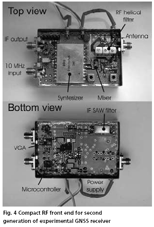
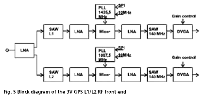
Compact designA natural process of design optimization led to the more compact RF front end (Fig. 4) for the second generation of experimental GNSS receiver. The intermediated frequency of this front end was increased to 140 MHz to improve suppression of the mirror reception. The helical IF filter was replaced by the SAW filter with much better form factor. The bandwidth of the filter is 16 MHz. The bandwidth of the signal can be further reduced by digital filter in receiver DSP if needed. The complete RF chain with microcontroller for synthesizer control was integrated into one box (50×70 mm) [Spacek (2005)]. The final step was development of the RF front end version for compact version of the receiver for GPS L1 and L2 frequency in euro card (100 x 160 mm) format. The designed compact RF front end has been again revised and 3V technology was used for all parts. The helical RF filters were replaced by the SAW filters. The hybrid synthesizers were replaced by the integrated ADF4360 by Analog Devices controlled by the external inductors. The more compactness of the design and use of unified 3V technology were paid by limited tuning possibility of the synthesizer and lesser flexibility of the design due to necessity of matching RF and IF amplifiers to 50 W. In the case of the use for the different navigation frequency the RF front end must be completely redesigned. The block diagram of such RF front end is in Fig. 5. SummaryThe concrete selection of the design method for RF front end depends on many factors like research aims, available technology and experiences. The simplest way how to design RF front end for experimentation with the GPS/GNSS signals is utilization of the RF front end of lot product receiver. This approach does not require many experiences with RF design. The features of the RF front end are done by manufacture and can be hardly fit to researcher requirements. More flexible approach is a design of the custom made RF front end. The design using GPS/GNSS RF ASIC is easier, but less flexible than the design based on universal RF components and integrated circuits. The most flexible solution is RF front end assembly from replaceable blocks. This approach enables easily modified RF front end characteristic in accordance with the application requirements.The modular design with validated parameters can be then optimized to the compact non-modifiable version. References• Parkinson KJ, Dempster AG, Muford P, Rizos C (2005). FPGA based GPS receiver design considerations. On the CD-ROM of the proceedings of International Symposium on GPS/GNSS 2005, The Hong Kong Polytechnic University, Hong Kong |
|||||||||||||||||||||||||||||
|
|||||||||||||||||||||||||||||
|
Pages: 1 2



 (No Ratings Yet)

